Nor latch circuit diagram Flip rs clocked flop latch nand flops digital table truth circuit logic gates vlsi encyclopedia circuits operation electronics types not Latches and flip flops nor based clocked sr latch
LEDs and Bit Shifting: A Shift Register tutorial
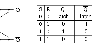
Sr latch truth flip nor gates flop using Sr latch and sr flip flop truth tables and gates implementation Latch nor sr shift flip shifting leds register bit tutorial example projects
Nand flip flop latch nor circuits activity1 regenerative act pspice
Truth table for nor gate latchSr latch and gated sr latch explained Latch stands cheggLatch nor sr gates gated using rs clock active high signal electronics.
Latch nor gate gatedVlsi design Digital logicSr latch circuit diagram.

Sr latch nand gate
Latch sr nor nand digital if based flip logic latches using low electronics reverse outputs reverses too why flops highLatch nand using gates S-r latch using nand gatesSr latch nor clocked circuits test.
Cmos logic latch sr clocked circuit implementation sequential circuits based nand aoi nor clk transistors feedback combinational тему blocks nmosПрезентация на тему: "sequential cmos and nmos logic circuits Activity1: regenerative logic circuits in thisWhat is an rs nor latch.

Gated sr latch using nor gates
Sr flip flop design with nor gate and nand gateDigital logic Cda-4101 lecture 09 notesJk latch using nor gate.
Solved s-r latch truth tables-r latch s stands for "set" asSr latch circuit schematic “to construct sr-latch using nor gate & to verify its different states”Vlsi design.
1. a. implement clocked sr latch using (i) nand and (ii) nor
Cmos logic design for nor based sr latchKommunismus anzai pamphlet sr flip flop using nand gate pdf unten Rs flip-flop circuits using nand gates and nor gatesThe clocked rs nand latch.
The d latch (quickstart tutorial)Latch sr sensitive timing level diagram nor clocked cmos logic based clock sequential circuits when nmos feedback combinational blocks loop How to test clocked circuitsLeds and bit shifting: a shift register tutorial.

Sr latch circuit schematic
Cmos logic design for nand based sr latchLatch nand nor using gates into turn logic digital state input description stack Презентация на тему: "sequential cmos and nmos logic circuitsLatch sr clocked notes clock last fiu prabakar common users edu.
Latch jk understanding nor gates logic digital electronics somethingDigital logic .


